Prerequisits
This project was set up with AMD/Xilinx Vivado in version 2023.2 and Vitis Classic 2023.2 under Ubuntu 20.04 using an Avnet UltraZed-3EG IO Carrier Card. Generally, the set-up described should also work in older and newer versions of Vivado and under other operating systems with similar Zynq UltraScale+ devices. Be aware that Windows 10/11 has problems running Makefiles which contain wildcard expressions such as *.c or *.h instead of the wildcard command of make. A fix for this can be found here.
Make sure to install picocom, which is used to communicate with the ARM processor on the evaluation board, using:
1
2
sudo apt update
sudo apt install -y picocom
And add yourself to the dailout group with:
1
sudo usermod -a -G dialout <YOUR_USERNAME>
Afterward, logout and login again such that the groups changes take effect.
Creating a Vivado project
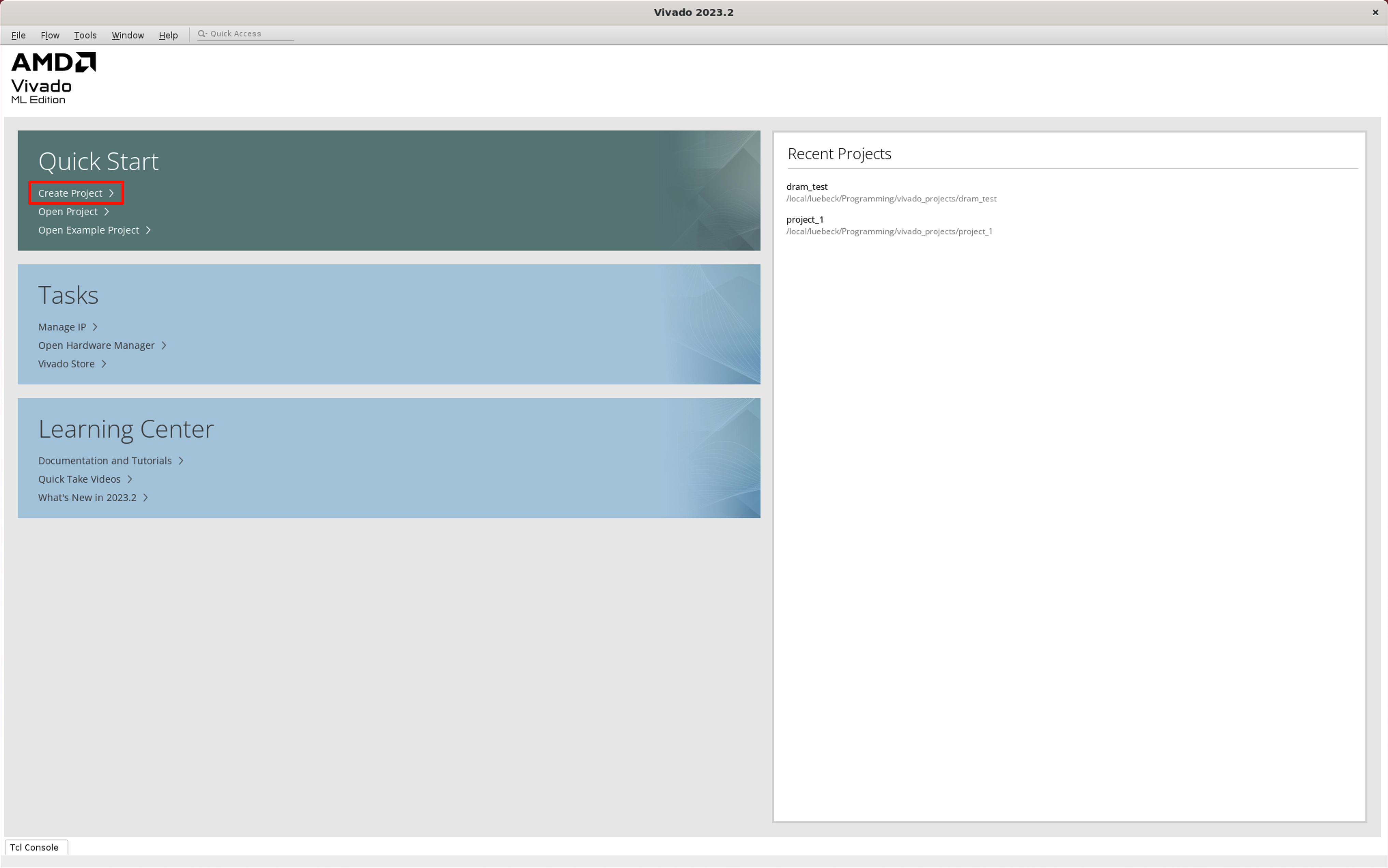
Start Vivado by clicking on its icon in the application menu. When Vivado has opened click on Quick Start -> Create Project
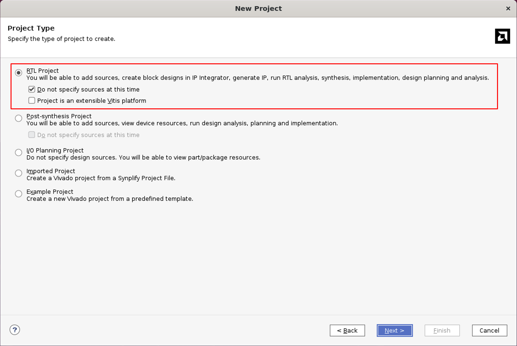
In the New Project dialog, click on Next and choose a project name and location. For this example project, set the project name axi_hello_world and click on Next. Choose RTL Project and check Do not specify sources at this time and uncheck Project is an extensible Vitis platform.
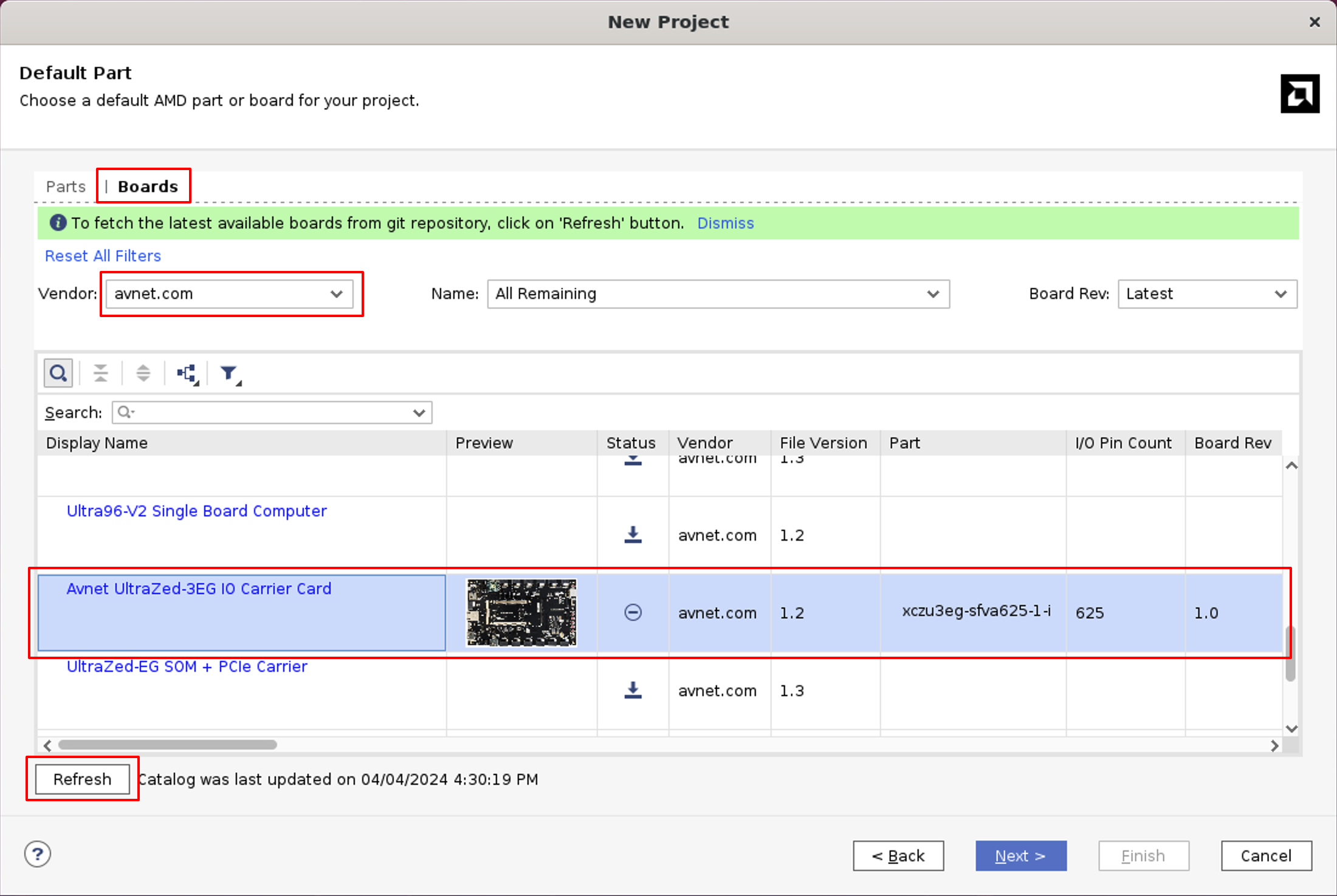
In the next step, you need to select the platform for which this project is intended. As this tutorial uses an Avnet evaluation board, choose Boards and then press Refresh to download the list of available boards from AMD/Xilinx. Then select the Vendor avnet.com from the drop-down menu and choose the matching board, for this tutorial this is the Avnet UltraZed-3EG IO Carrier Card. If you haven’t downloaded the board files yet, click on the download symbol in the Status column and press Next to continue.
Finish the Vivado project creation by pressing Finish.
Create a Synthesizable Vivado Block Design
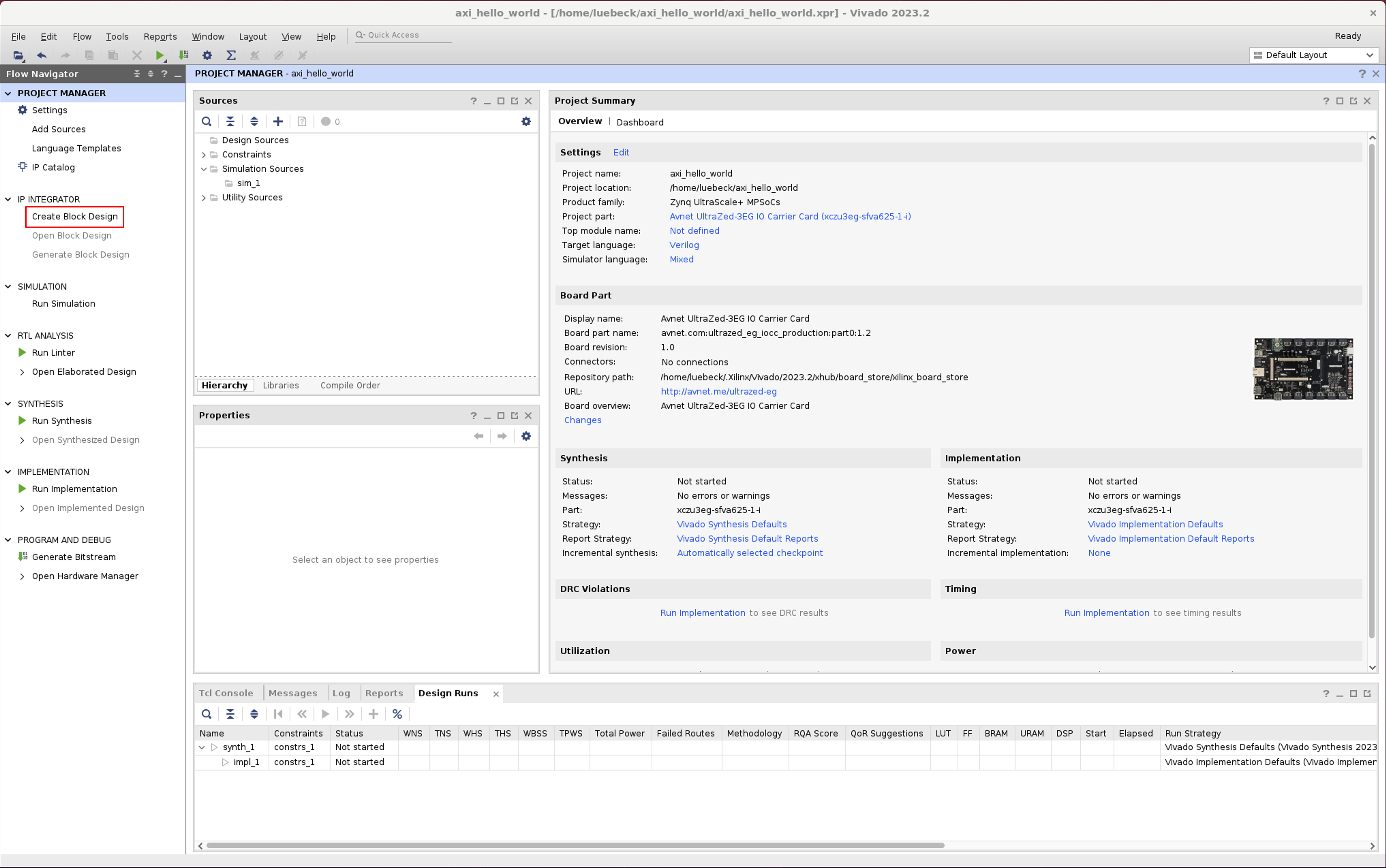
After the project creation is finished, Vivado presents you with a project overview. To implement anything on the FPGA (also called PL, for Programmable Logic) a Block Design needs to be created. In the Flow Navigator -> IP Integrator press Create Block Design.
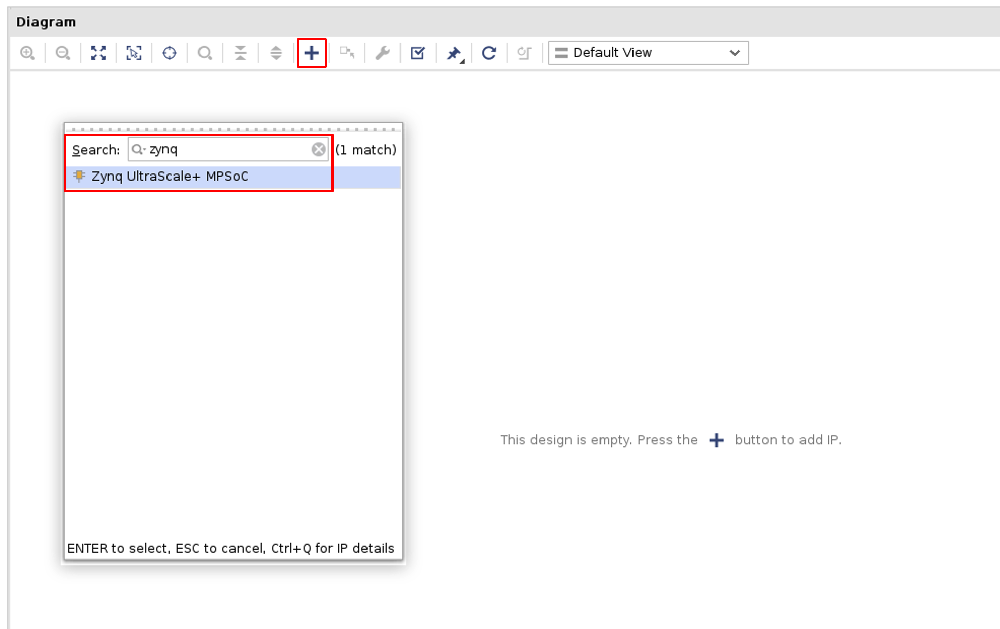
In the Create Block Design dialog, leave the Design name at design_1 and press OK. In the Diagram view press on the + icon to add an IP block. The first IP block that needs to be added is the Zynq UltraScale+ MPSoC, double-click on it to add it to the block design.
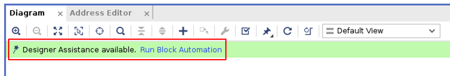
Vivado is now providing some help to configure the Zynq IP block, Click on Run Block Automation.
In the Run Block Automation dialog, check All Automation and Apply Board Preset and press OK.
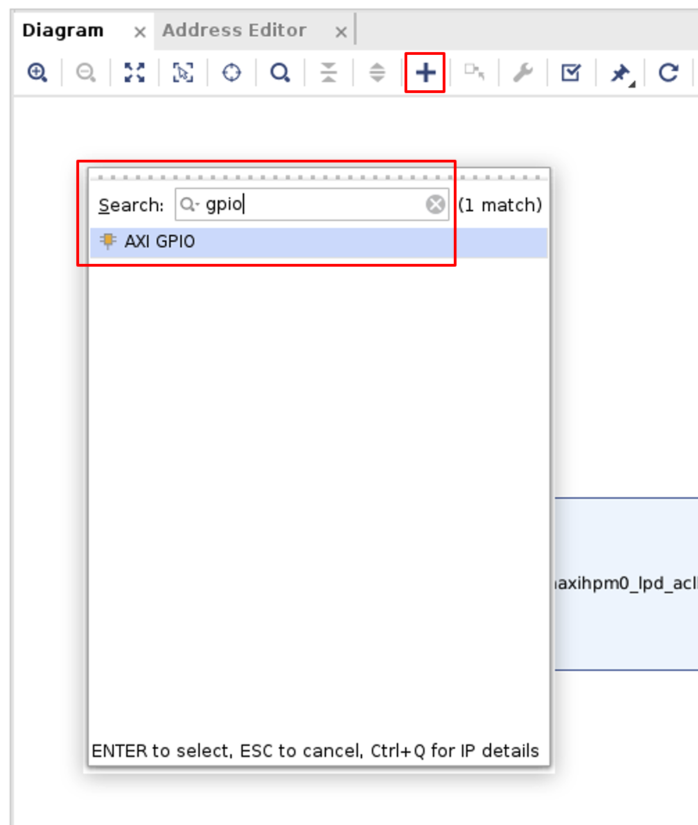
Afterward, an AXI IP that can address the GPIO pins connected to the PL-LEDs needs to be added. Press + to add another IP block and search for AXI GPIO and double-click on it to add it to the block design.
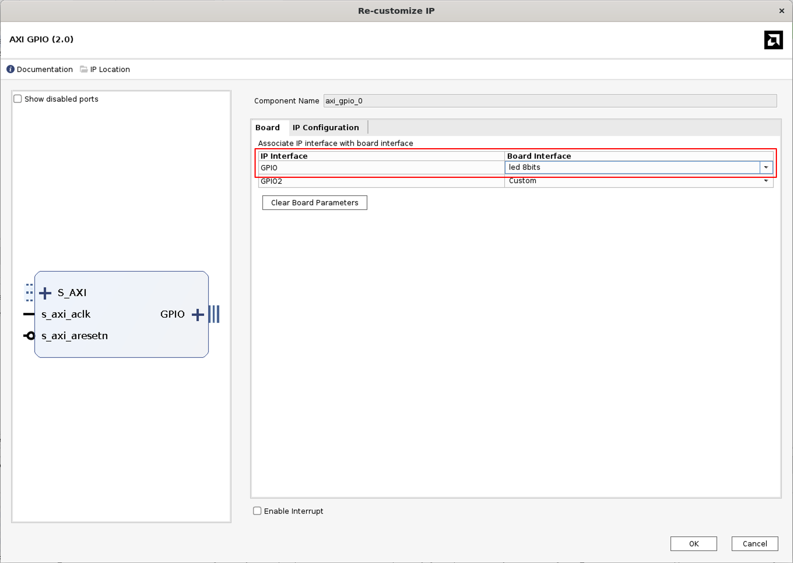
When the AXI GPIO block has been added to the block diagram, double-click on the newly added block to configure it. In the Re-customize IP dialog, set GPIO to led 8bit and press OK.
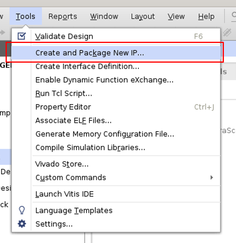
To make this tutorial a bit more interesting another custom AXI IP block will be added. In the Vivado menu, choose Tools -> Create and Package New IP.
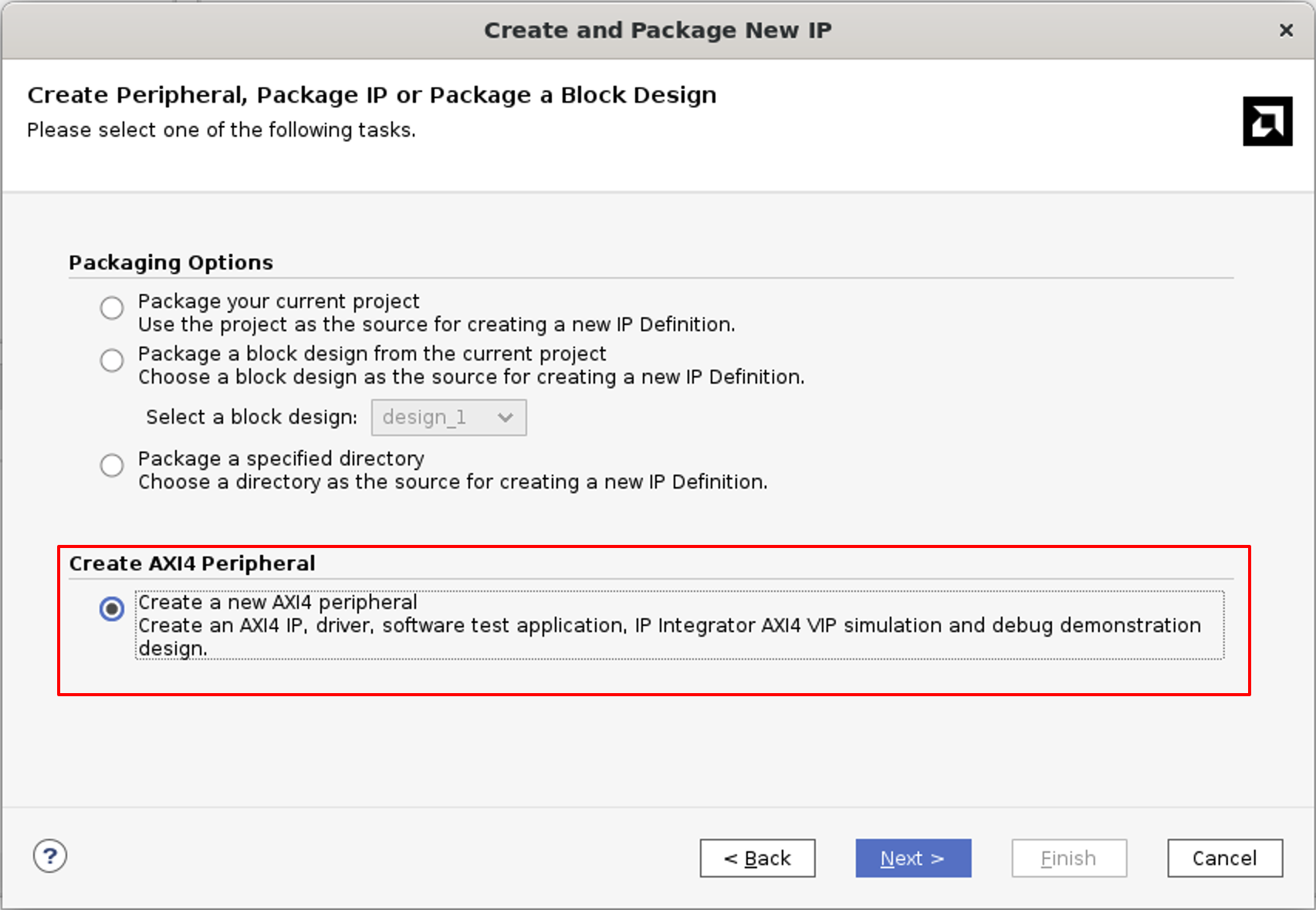
In the Create and Package new IP dialog, press Next, then choose Create AXI4 Peripheral and press Next.
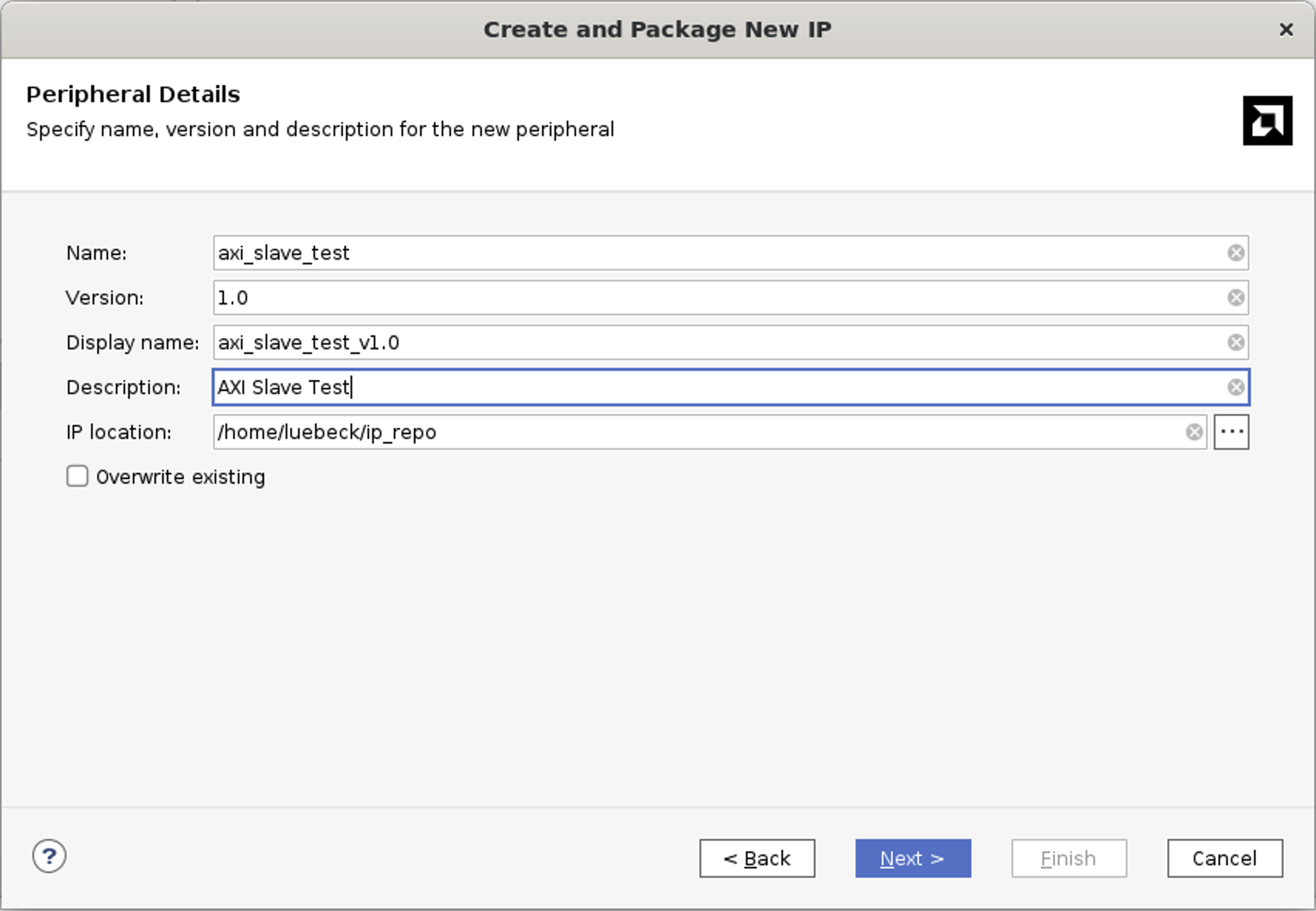
Set the Name axi_slave_test, and Description AXI Slave Test and press Next.
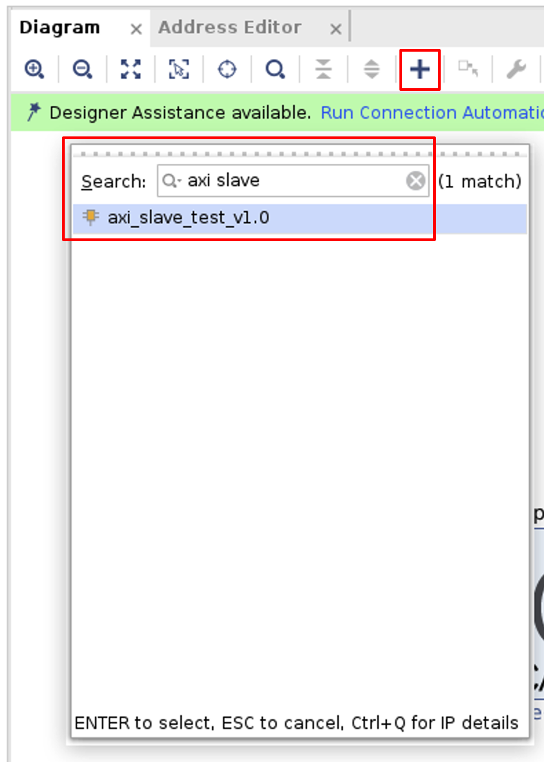
In the next step leave everything at the default settings and press Next and then choose Add IP to the repository and press Finish. This AXI Slave Test IP can now be added to the block design. Press on the + icon in the block design diagram and search for the AXI Slave Test to add it.
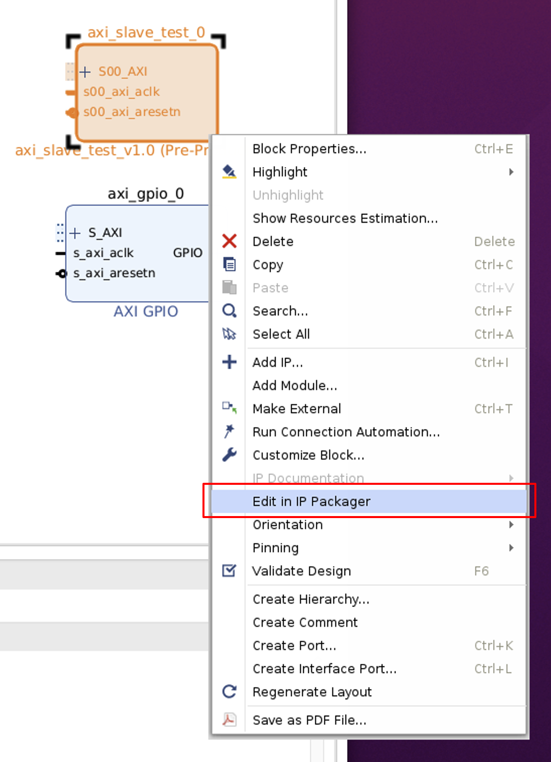
When the AXI Slave Test was added to the block design, the Verilog code of it can be customized. Right-click on the axi_slave_test_0 block and select Edit in IP Packager.
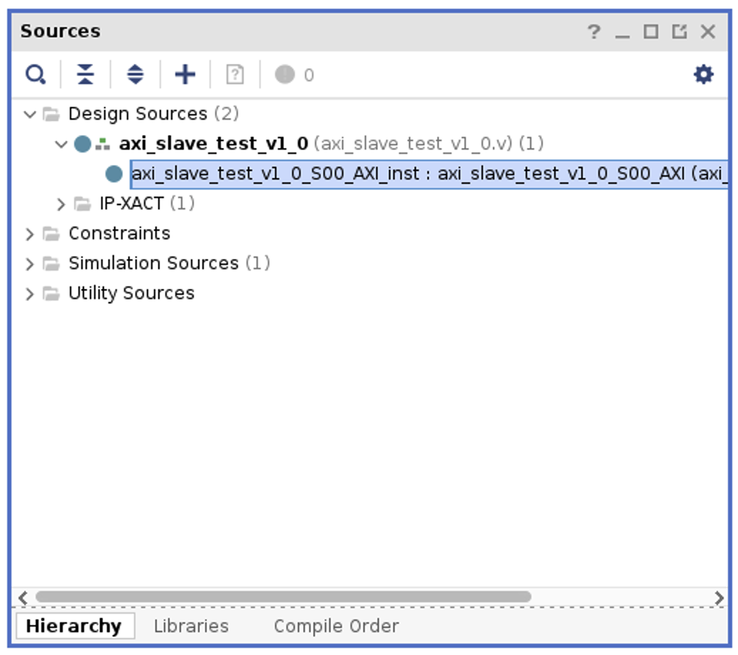
In the Edit in IP Packager leave everything at the default settings and press OK. Now a second Vivado window opened in which the Verilog code of the AXI Slave Test can be edited. In the Sources tree navigate to Design Sources -> axi_slave_test_v1_0 -> axi_slave_test_v1_0_0_S00_AXI_inst ... and double-click it.
In the Verilog file axi_slave_test_v1_0_0_S00_AXI.v you can see the complete logic of an AXI Lite Slave. This slave allows you to write to the registers slv_reg0 to slv_reg3 using memory mapped IO on the ARM CPU (PS). Currently, the register values do not trigger an action or change the data written to the registers. For the purpose of this tutorial slv_reg3 should always return 0xdeadbeef when reading from it and slv_reg0 should return the written value increased by 1.
Firstly, the write logic for slv_reg3 needs to be commented out (line 253 to 259).
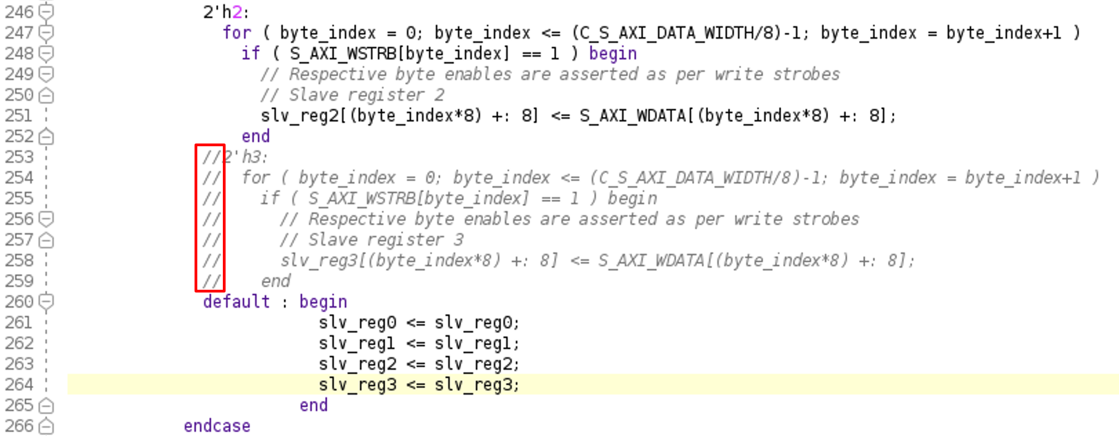
Secondly, the value of slv_reg3 must be set to 32'hdeadbeef when the AXI Slave is reset (line 226).

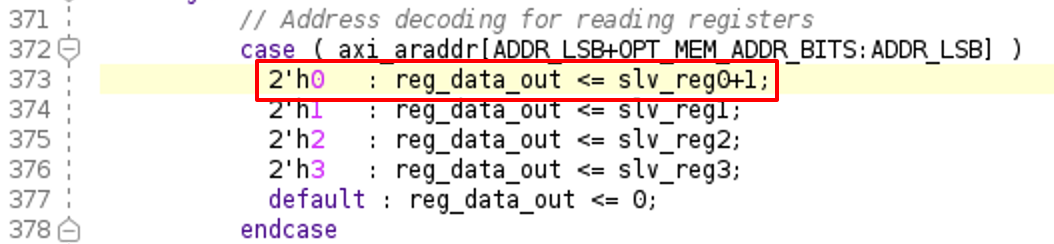
To increase the value of slv_reg0 by 1 when reading from the register, add a +1 to line 373.
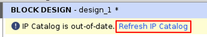
When you finished editing the Verilog code save it by pressing [CTRL]+[S] and close the Vivado window in which the AXI Slave Test was edited in. In the Vivado window in which the block design is opened, the message IP Catatlog is out-of-date should appear. Press Refresh IP Catalog to update it with the changes that have been applied to AXI Slave Test.
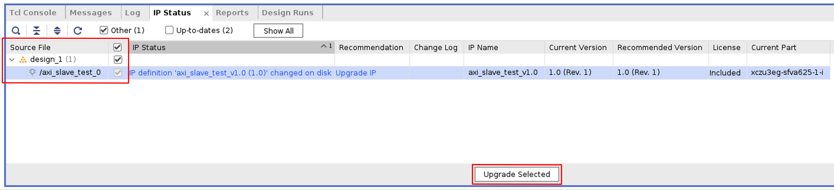
Below the block design diagram, the IP Status will appear. Make sure to select the axi_slave_test_0 and press Upgrade Selected and press Skip when asked to Generate Output Products.
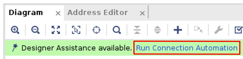
Now, two AXI slaves are in the block design diagram. However, they aren’t connected to the ARM CPU (PS), to do this use the connection automation by clicking on Run Connection Automation.
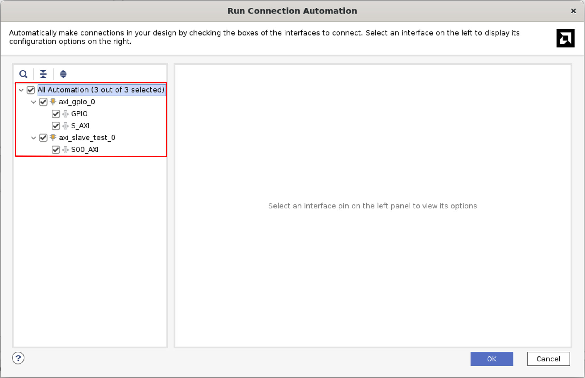
In the Run Connection Automation dialog check All Automation such that all blocks get connected to each other and press OK.
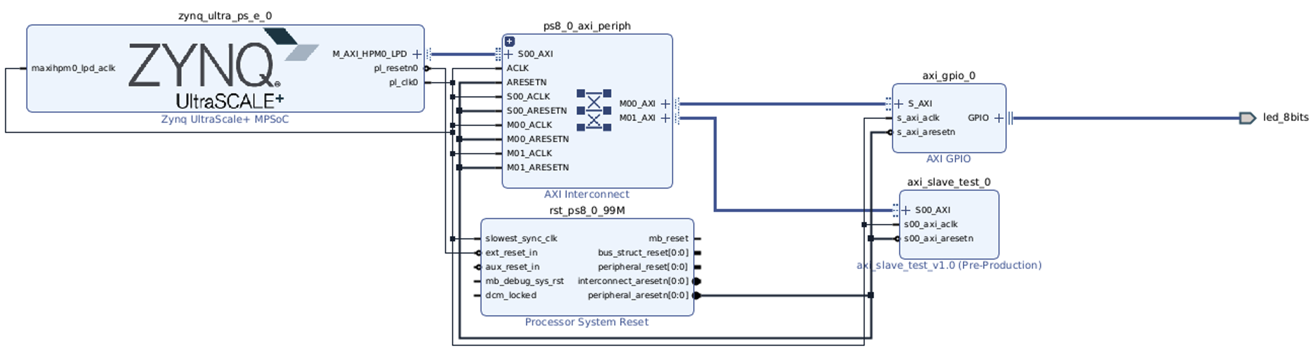
Afterward, the block design diagram should look like the following image (the individual blocks can be at different locations, but the wires should match).
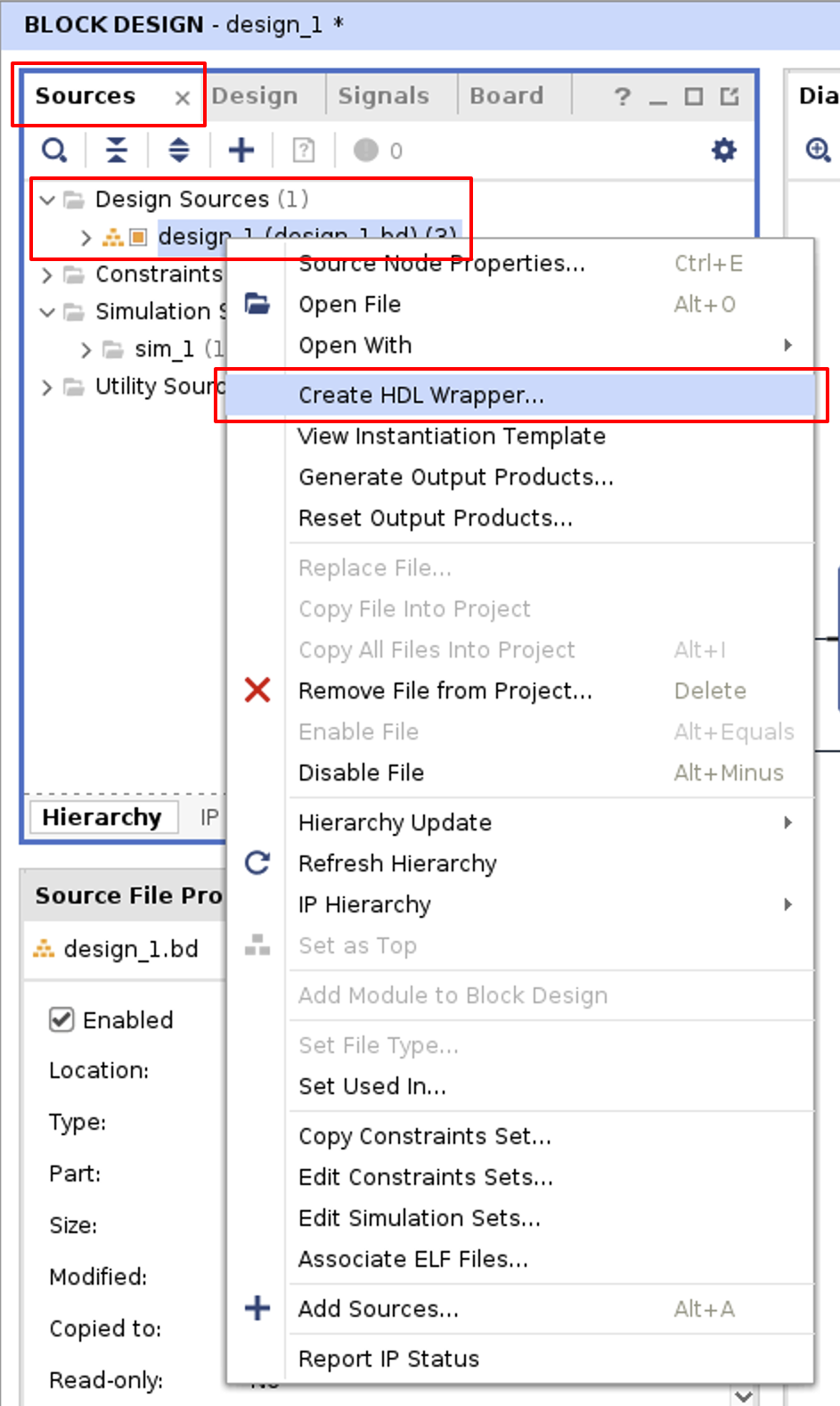
To be able to synthesize the block diagram and generate a FPAG bitstream, Verilog code needs to be generated. This can be done by Vivado automatically. In the block design view, go to Sources on the left-hand side, unfold Design Sources right-click on design_1 (this would be named differently if you set a different name for the block design) and choose Create HDL Wrapper.
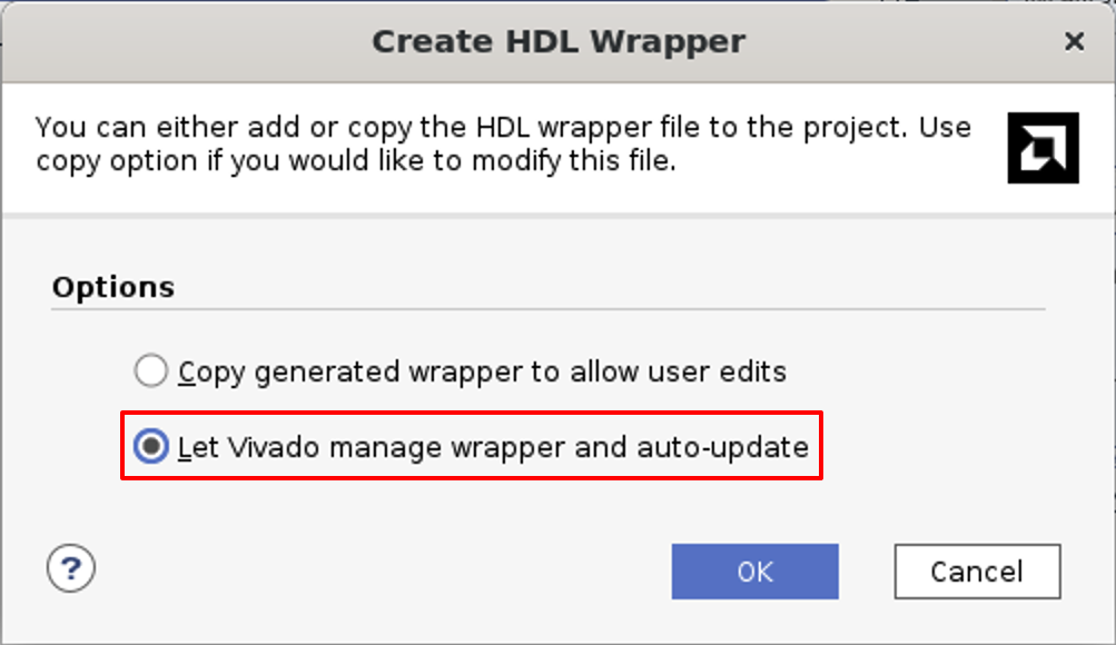
In the Create HDL Wrapper dialog, select Let Vivado manage wrapper and auto-update and press OK.
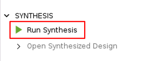
With the block design completed it can now be synthesized. In the Flow Navigator on the left-hand side unfold Systhesis and press Run Synthesis.
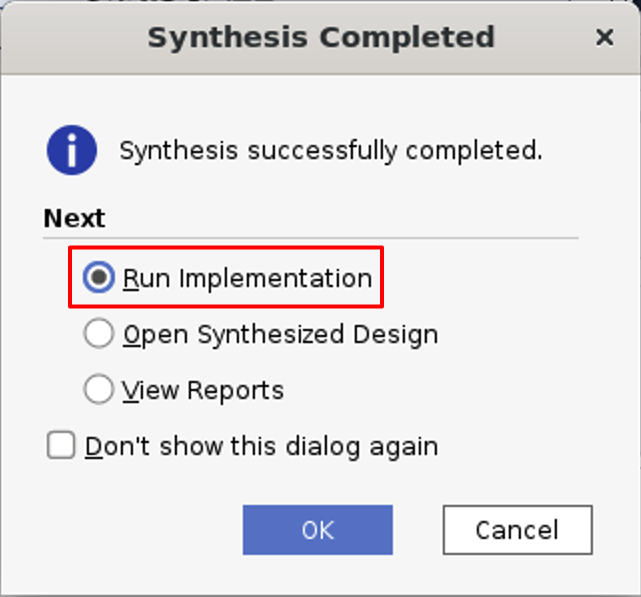
In the Launch Runs dialog, leave everything at its default and press OK. Depending on your hardware, the synthesis could take a couple of minutes. When the synthesis has finished, you are presented with the Synthesis Completed dialog. Select Run Implementation and press OK to implement the synthesized design, which will place and route everything for the FPGA.
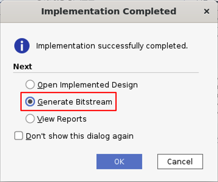
The Launch Runs dialog will appear again, leave everything at its default and press OK. When the implementation has completed, you are presented with the Implementation Completed dialog, select Generate Bitstream and press OK.
The Launch Runs dialog will appear a third time, leave everything at its default and press OK. When the bitstream generation completed the Bitstream Generation Completed appears, you can press Cancel as the floor plan etc. is not relevant at the moment.
This concludes the creation of a Vivado project and implementing a block design for the PL. The next step is the implementation of the software on the PS (ARM CPU).
Implementing a C Program to Communicate with the FPGA (PL) Design using Vitis Classic
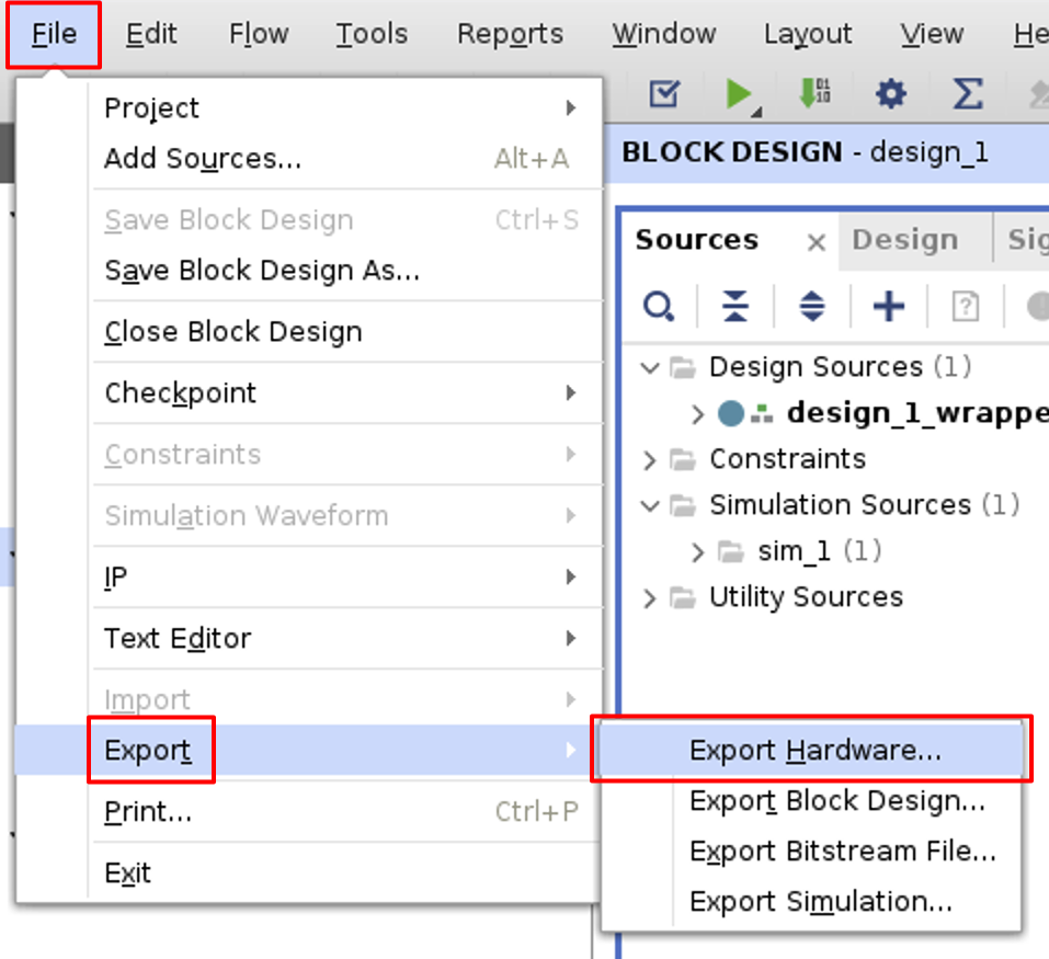
When the bitstream has been generated go to the Vivado menu and choose File -> Export -> Export Hardware
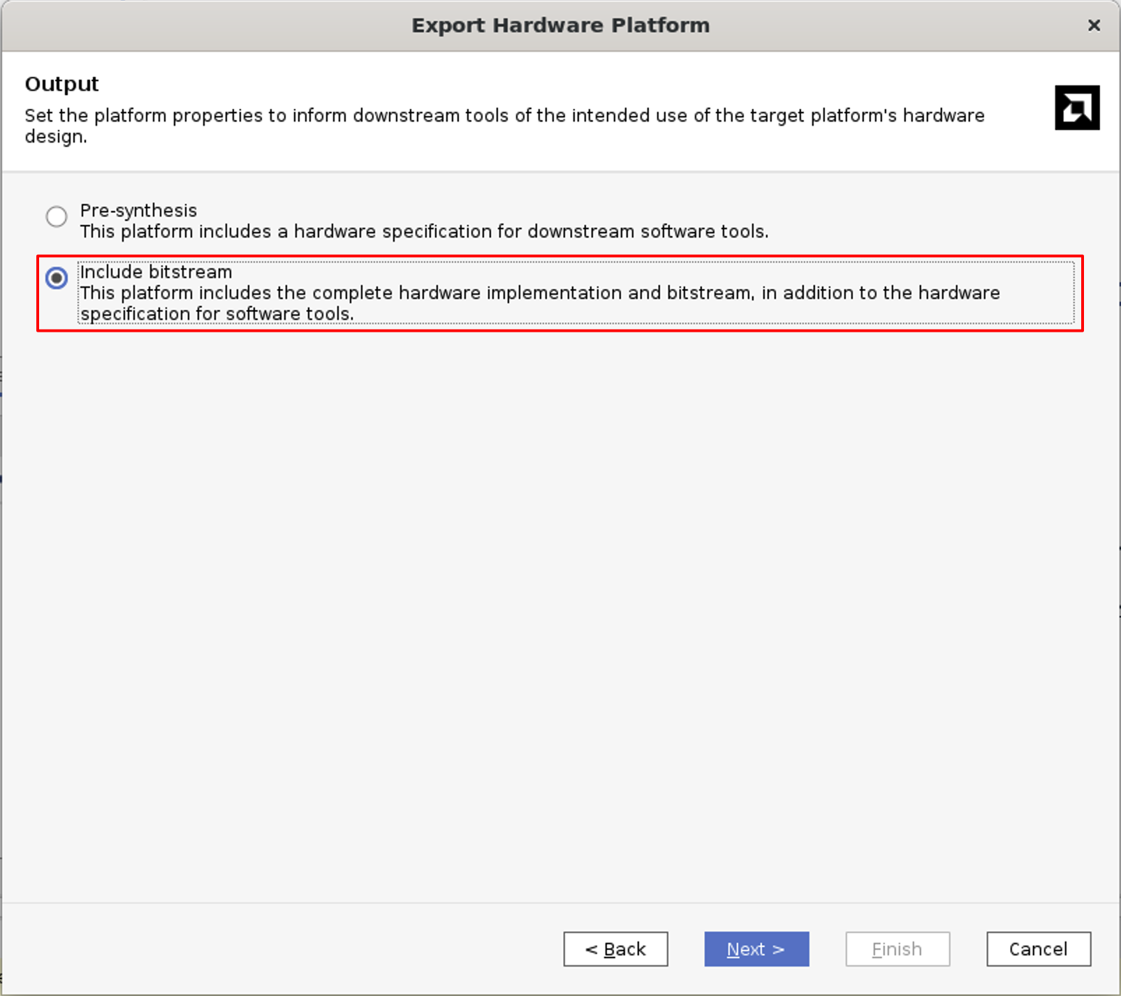
In the Export Hardware Platform dialog press Next and on the next step select Include Bitstream and then press Next.
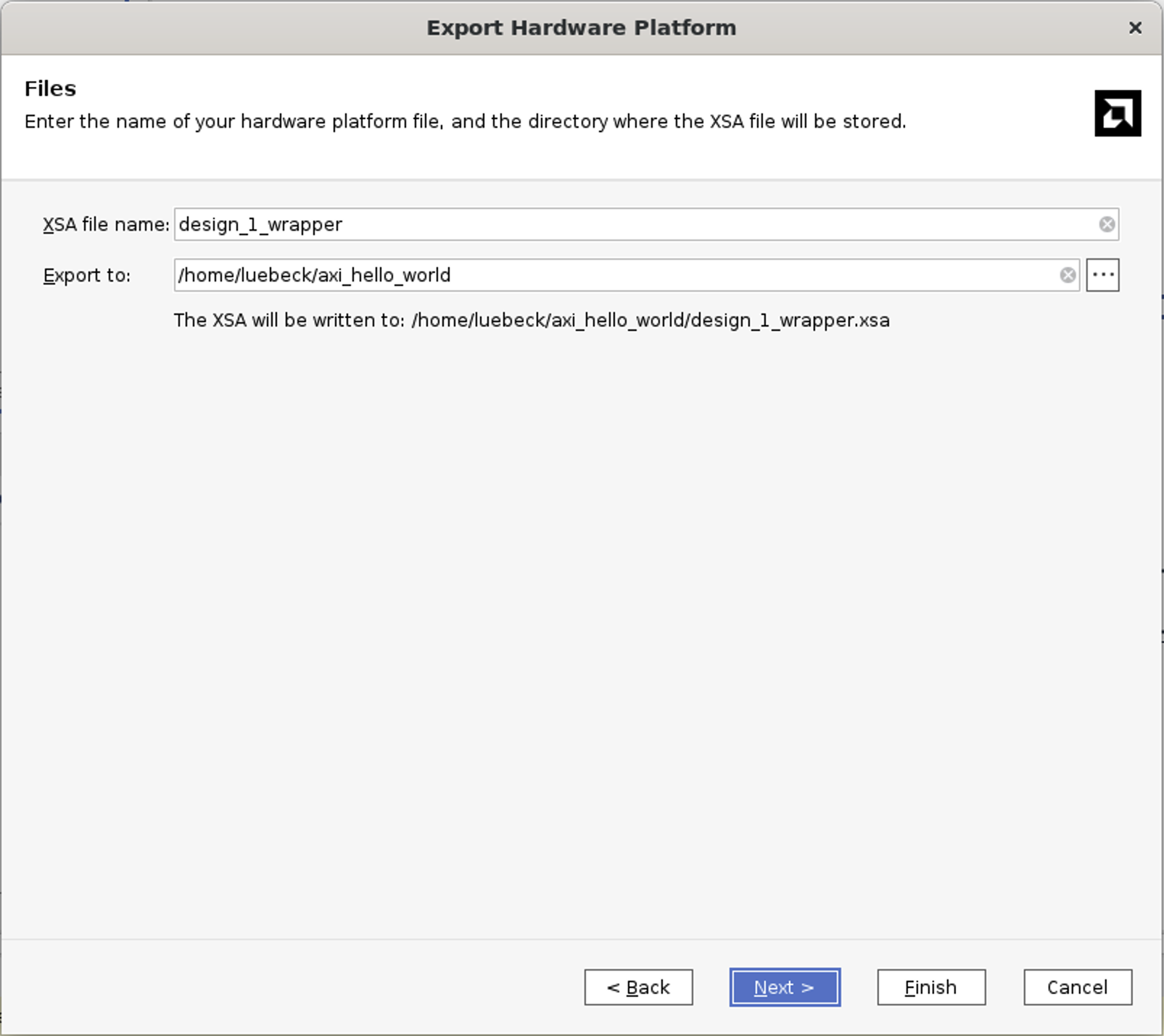
In the next step of the Export Hardware Platform dialog, leave the XSA file name and Export to path at their default values and press Next and then Finish. The XSA file and the path to it is later on needed in Vitis to set up the C code project.
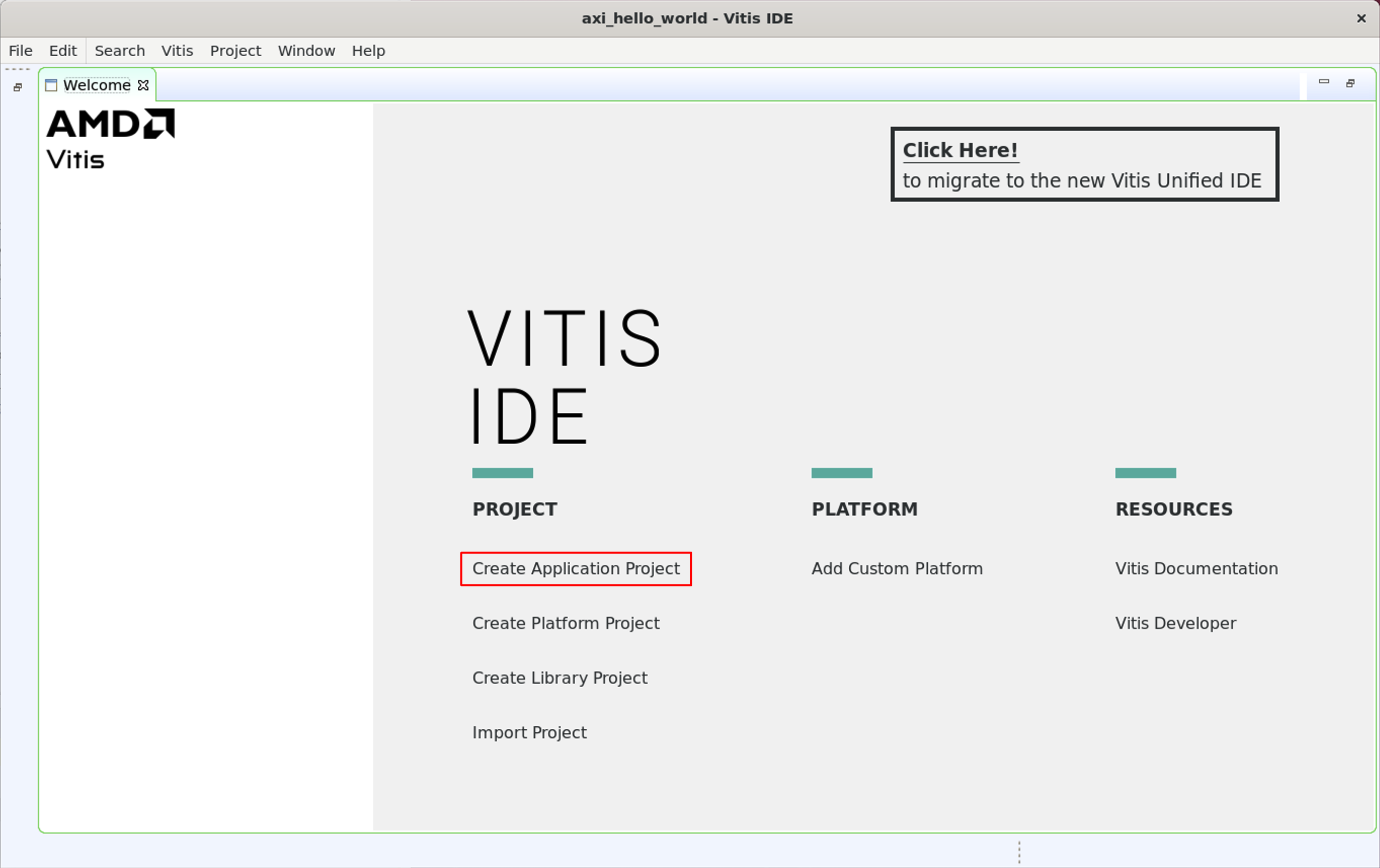
Now open Vitis Classic and choose a path for your workspace this is the path where all your Vitis projects will be stored and then press Launch. I create a new workspace for every Vivado project, but that is up to your preference.
In the Vitis overview, press Create Application Project.
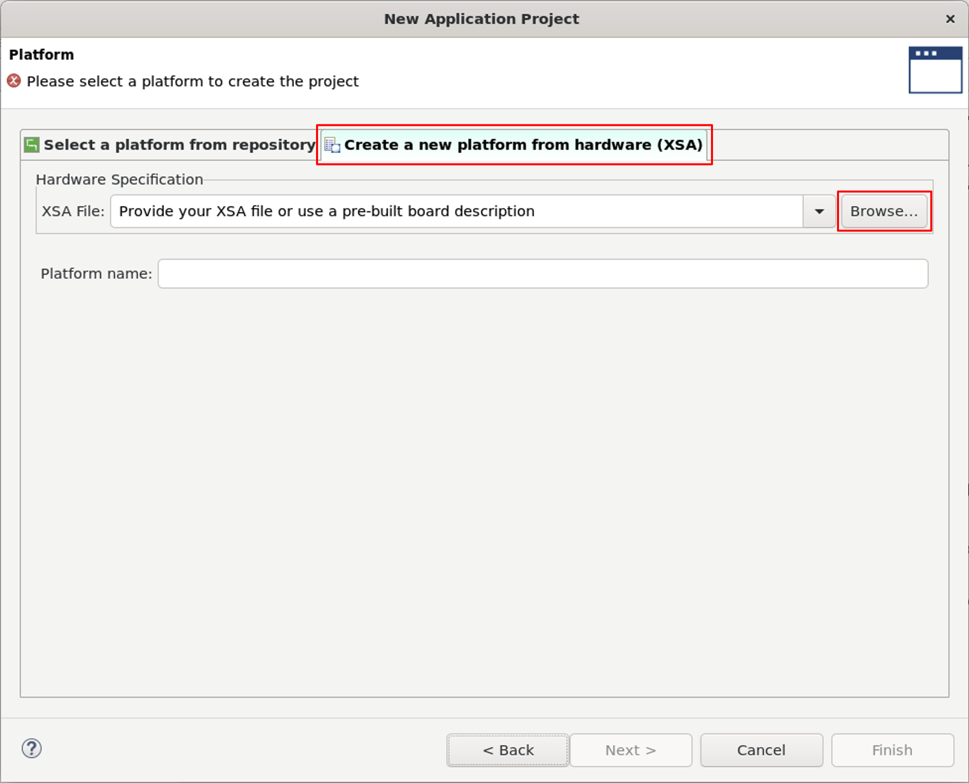
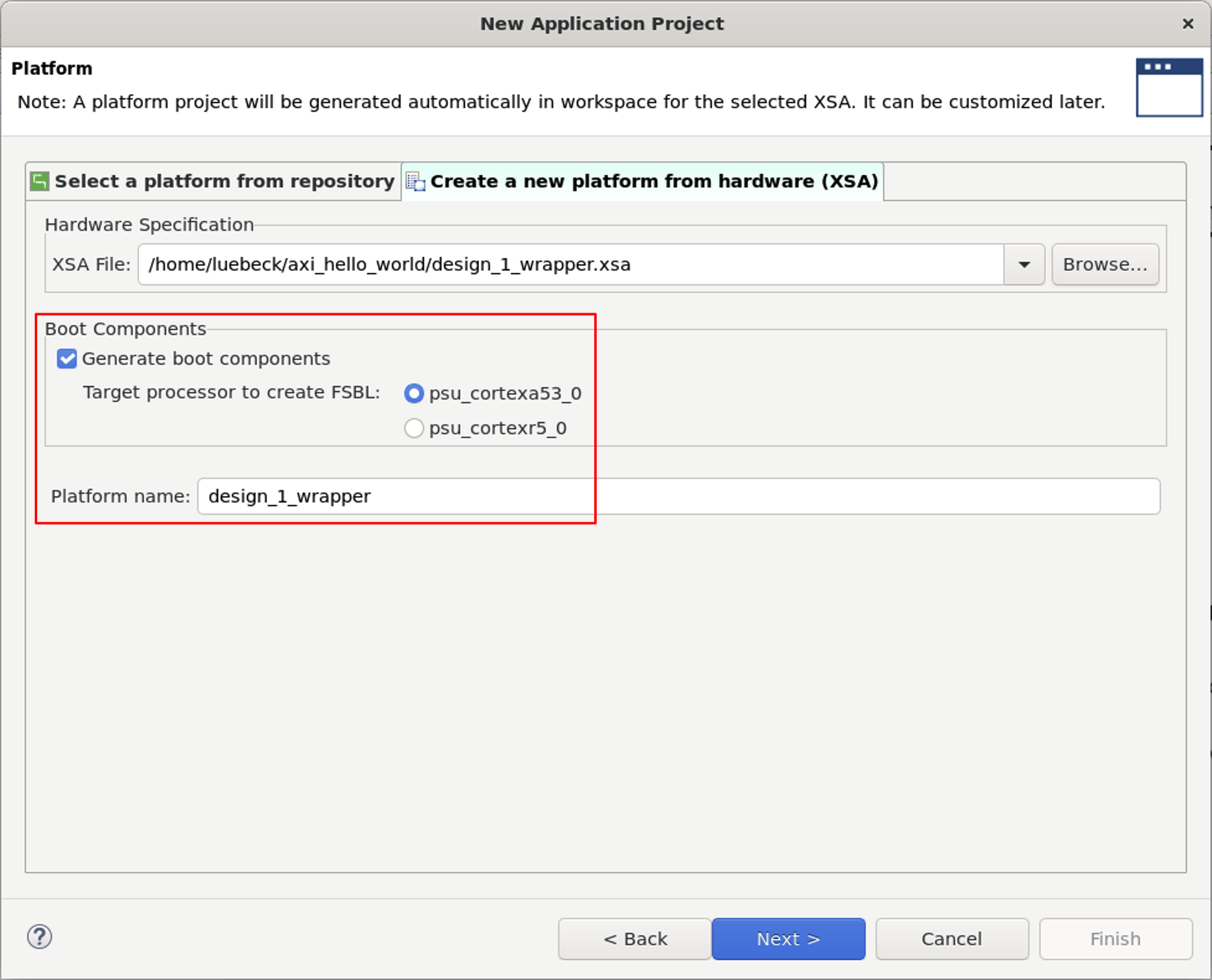
In the first step of the New Application Project dialog press Next. In the second step select the tab Create a new platform from hardware (XSA) and press Browse and select the XSA file exported in Vivado and leave the settings for Boot Components at its default values and then press Next.
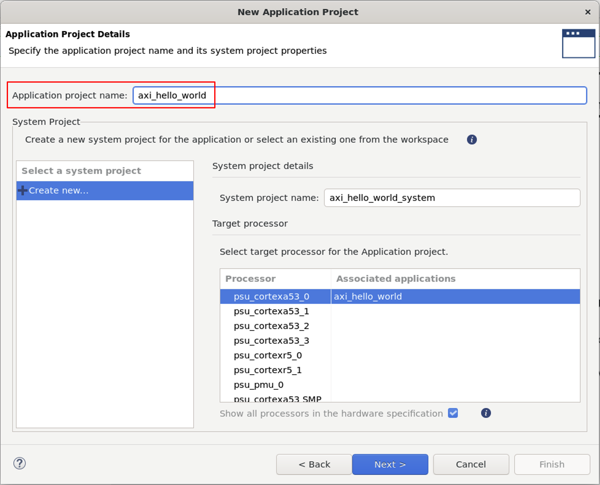
Next, set an Application project name, for this tutorial set it to axi_hello_world, and leave everything else at its default settings and press Next.
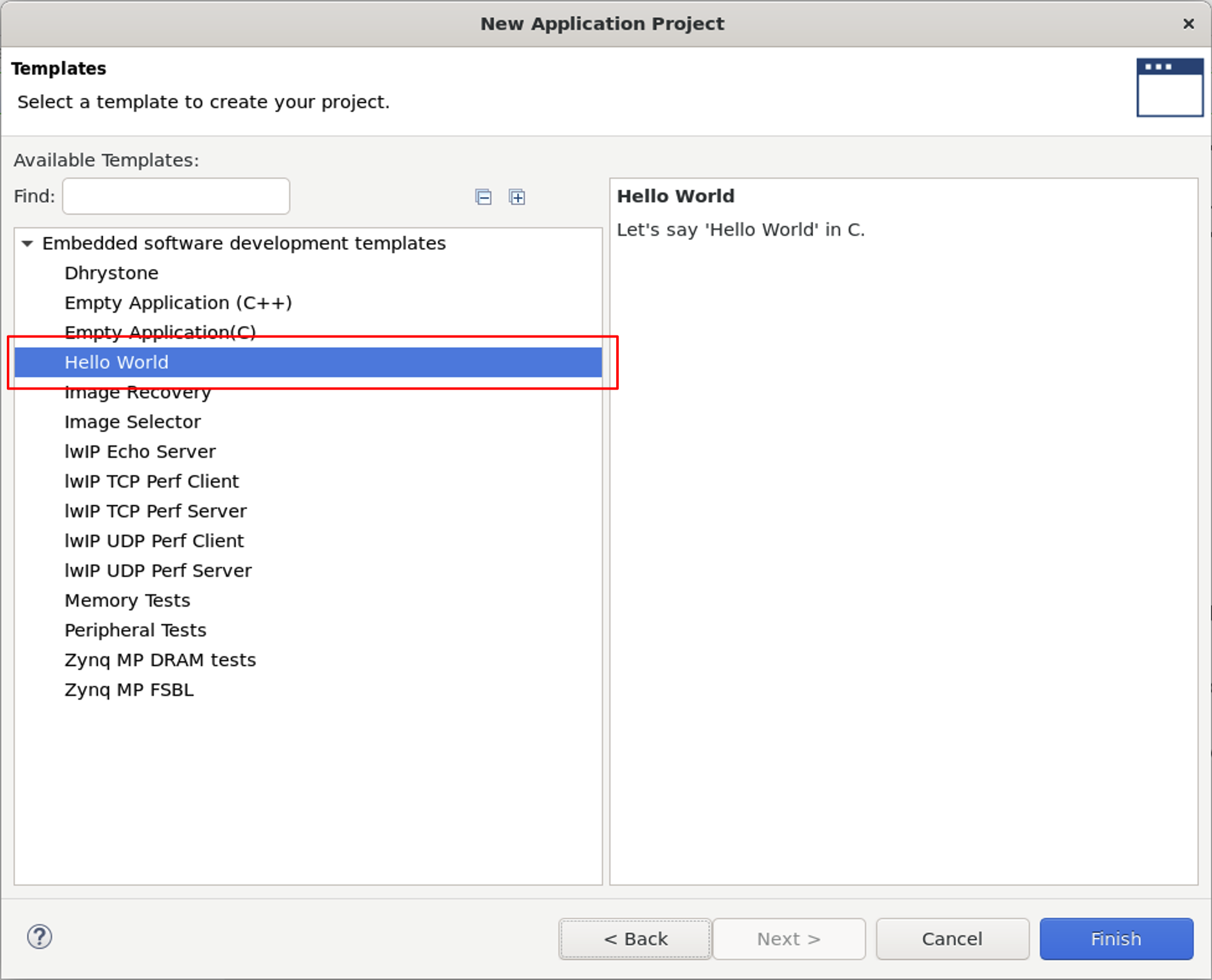
In the next step of the New Application Project dialog, press Next without changing anything. In the last step, select the Hello World template and press Finish.
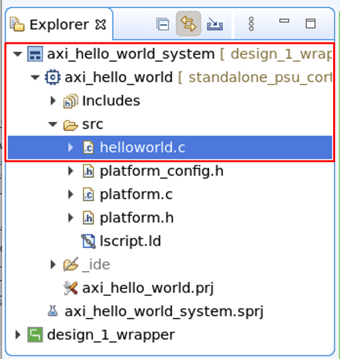
Now there are two projects in Vitis axi_hello_world_system and design_1_wrapper. The axi_hello_world_system is the project containing your code while the design_1_wrapper contains all libraries to compile your project. To get to the main function of the example Hello World program unfold axi_hello_world_system -> axi_hello_world -> src -> helloworld.c
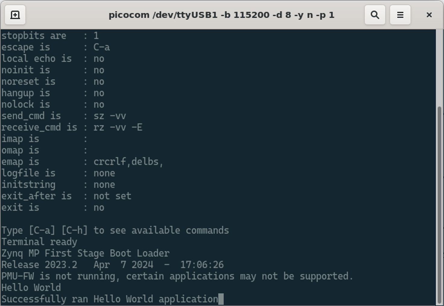
To test that creating the project was successful, build it the first time by pressing the build icon (hammer), while the helloworld.c file is opened and currently in focus. If the build was successful, you are going to see the message Finished building: axi_hello_world.elf.size in the Console below the code view. The program you just built runs bare-metal on the ARM CPU (PS) and sets up the CPU using init_platform() prints Hello World and Sucessfully ran Hello World application through the UART and then ends itself.
Before running the Hello World program, connect the UltraZed board to power and the DUAL USB UART and the SMT3 JTAG using micro USB cables to your computer.
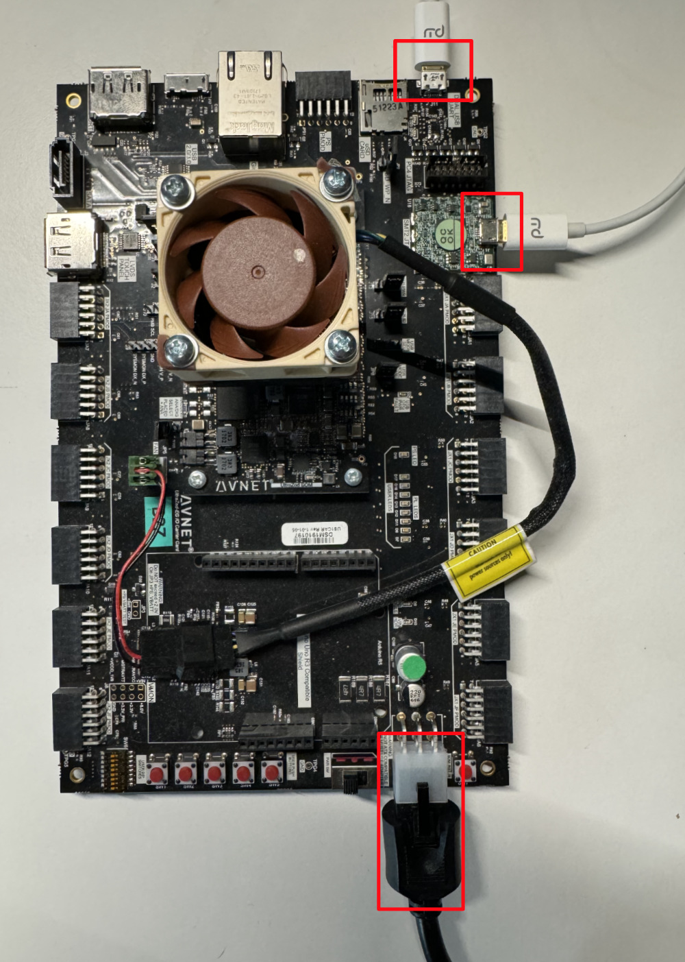
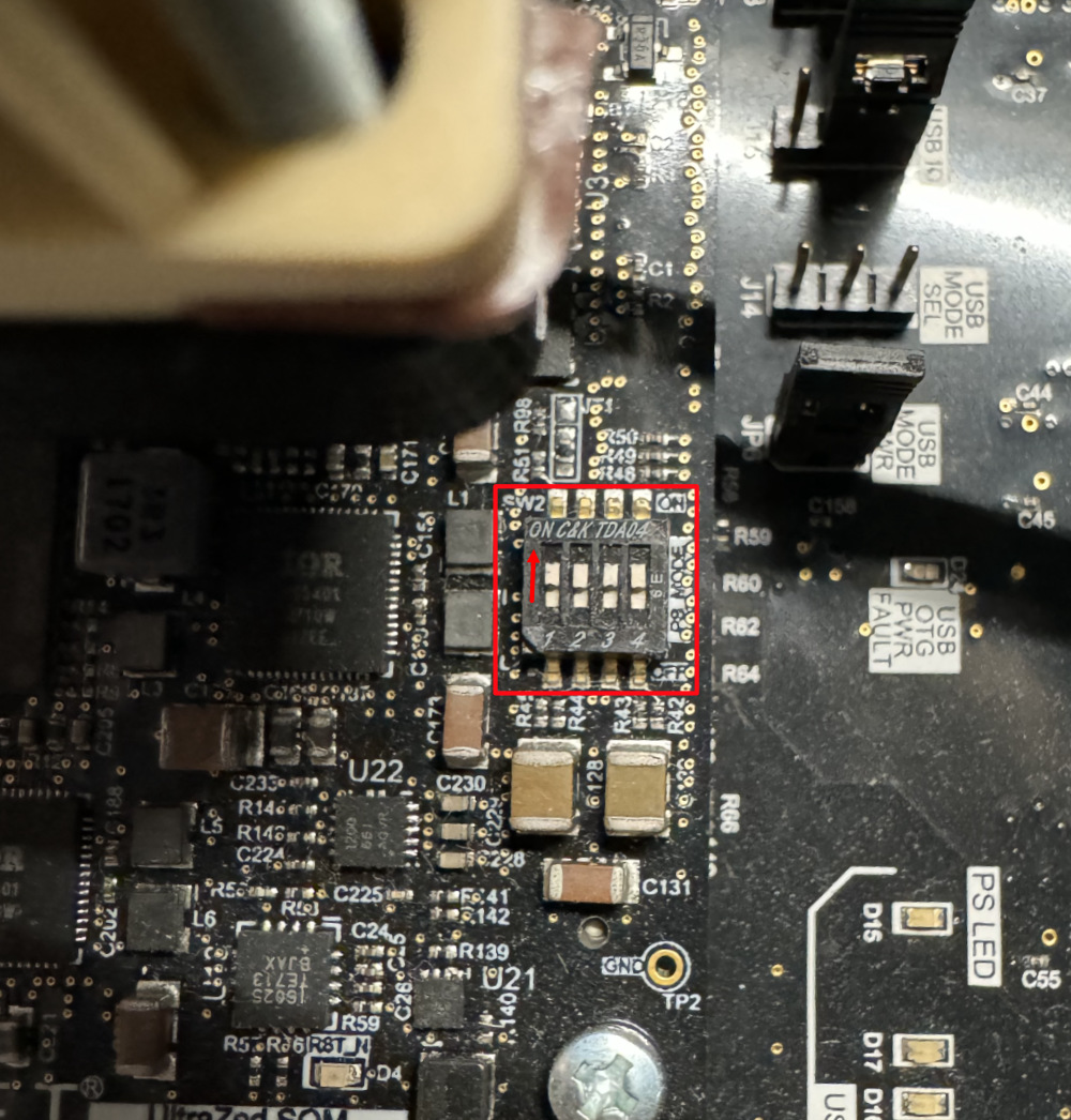
Before turning the board on, make sure the dip switch SW2 is set to ON-ON-ON-ON which set the bootloader into bare-metal mode.
Now turn the board on and then open a terminal and use picocom to connect to the UART of the UltraZed board using the following command:
1
picocom /dev/ttyUSB1 -b 115200 -d 8 -y n -p 1
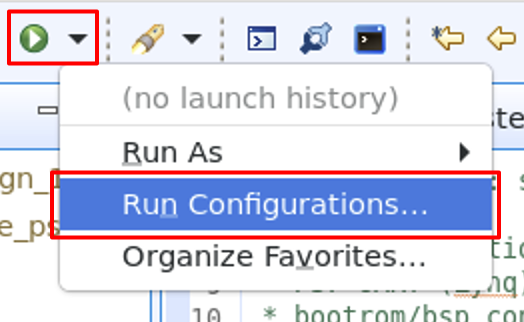
Now you are almost ready to run the Hello World program on the ARM CPU (PS) of the UltraZed board. Click on the drop-down menu right of the run icon and choose Run Configurations.
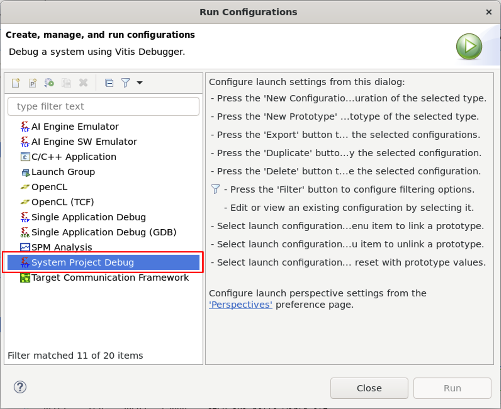
In the Run Configurations dialog double-click on System Project Debug.
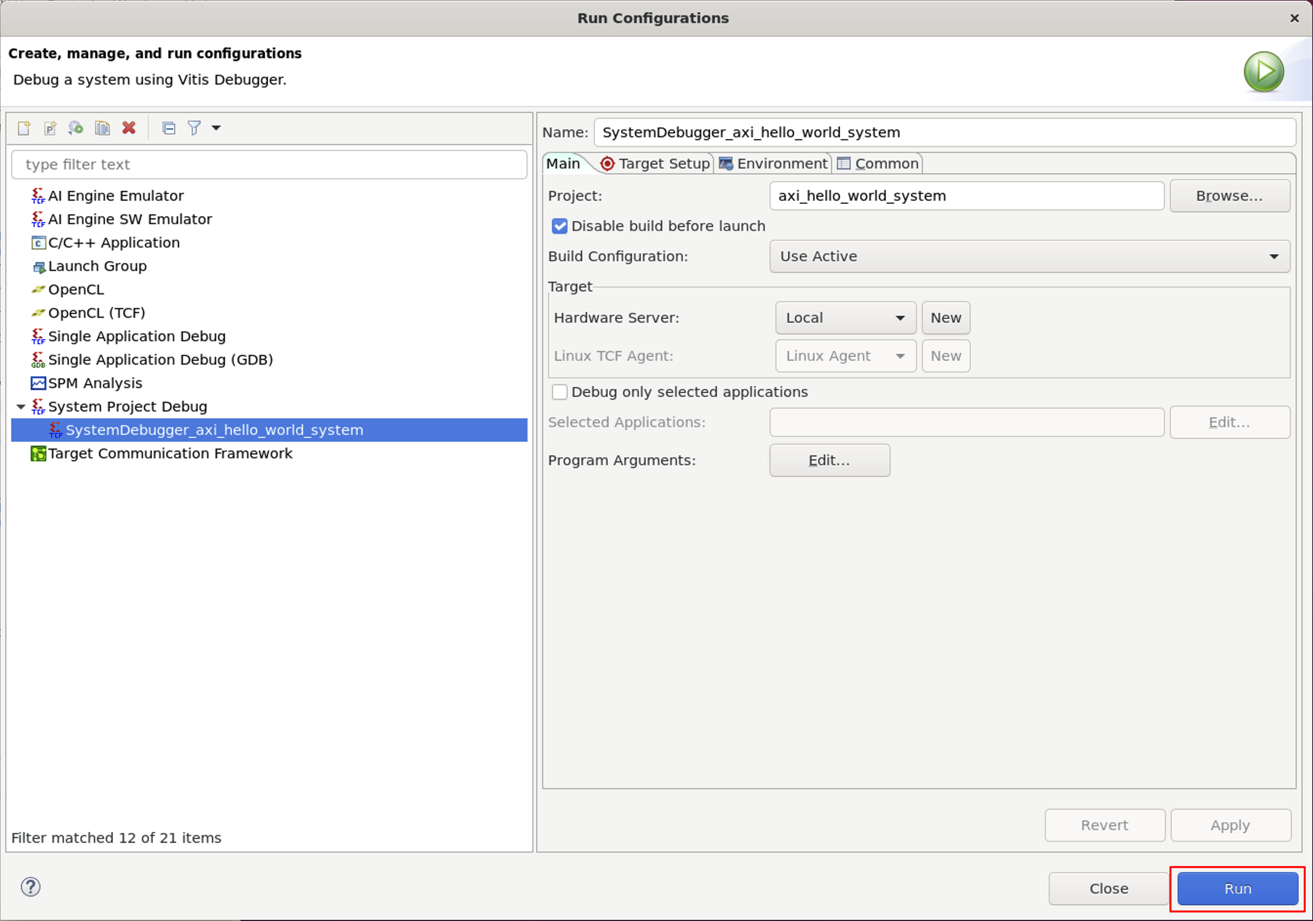
The newly opened run configuration in the Run Configurations can now be run by pressing Run. This will load the bitstream onto the FPGA (PL) and load the compiled code onto the ARM CPU (PS) and starts executing it.
When the Hello World program ran successful you will see the following message in the terminal:
Communicating with the AXI Slaves on the PL using C Code
The last step is to change the C code to communicate with the two AXI slaves added to the block design in Vivado. Each AXI slave has registers which can be addressed through memory mapped IO. Since the C code runs bare-metal, there are no virtual addresses and the physical addresses of the AXI slaves can be found in the xparameters.h header file. Add the following line to the includes of helloworld.c:
1
#include "xparameters.h"
And then press [CTRL] and click on the newly added line to open the xparameters.h file. In the header file you can find a section dedicated to the AXI Slave Test which you generated and modified in Vivado:
1
2
3
4
5
6
7
8
/******************************************************************/
/* Definitions for driver AXI_SLAVE_TEST */
#define XPAR_AXI_SLAVE_TEST_NUM_INSTANCES 1

/* Definitions for peripheral AXI_SLAVE_TEST_0 */
#define XPAR_AXI_SLAVE_TEST_0_DEVICE_ID 0
#define XPAR_AXI_SLAVE_TEST_0_S00_AXI_BASEADDR 0x80010000
#define XPAR_AXI_SLAVE_TEST_0_S00_AXI_HIGHADDR 0x8001FFFF
The important definition in this block is XPAR_AXI_SLAVE_TEST_0_S00_AXI_BASEADDR which is the address of the slv_reg0 of the AXI Slave Test. To access and modify the register values add the include #include "xbasic_types.h after #include "xparameters.h" to the helloworld.c and the following code block after the Hello World print:
1
2
3
4
5
6
7
8
9
10
11
12
13
14
15
16
17
18
19
20
21
22
23
// Address AXI slave test
volatile Xuint32* axi_slave_test_baseaddr_p = (Xuint32*) XPAR_AXI_SLAVE_TEST_0_S00_AXI_BASEADDR;

volatile Xuint32* axi_slave_test_reg_0_p = axi_slave_test_baseaddr_p;
volatile Xuint32* axi_slave_test_reg_1_p = axi_slave_test_baseaddr_p+1;
volatile Xuint32* axi_slave_test_reg_2_p = axi_slave_test_baseaddr_p+2;
volatile Xuint32* axi_slave_test_reg_3_p = axi_slave_test_baseaddr_p+3;

xil_printf("READ: axi_slave_test_reg_0 0x%x\n\r", *axi_slave_test_reg_0_p);
xil_printf("READ: axi_slave_test_reg_1 %d\n\r", *axi_slave_test_reg_1_p);
xil_printf("READ: axi_slave_test_reg_2 %d\n\r", *axi_slave_test_reg_2_p);
xil_printf("READ: axi_slave_test_reg_3 0x%x\n\r", *axi_slave_test_reg_3_p);

xil_printf("WRITE\n\r");
*axi_slave_test_reg_0_p = 0xFF00FF00;
*axi_slave_test_reg_1_p = 23;
*axi_slave_test_reg_2_p = 42;
*axi_slave_test_reg_3_p = 37;

xil_printf("READ: axi_slave_test_reg_0 0x%x\n\r", *axi_slave_test_reg_0_p);
xil_printf("READ: axi_slave_test_reg_1 %d\n\r", *axi_slave_test_reg_1_p);
xil_printf("READ: axi_slave_test_reg_2 %d\n\r", *axi_slave_test_reg_2_p);
xil_printf("READ: axi_slave_test_reg_3 0x%x\n\r", *axi_slave_test_reg_3_p);
This C code block assigns the registers slv_reg0 to slv_reg3 of the AXI Slave Test to the axi_slave_test_reg_0_p to axi_slave_test_reg_3_p pointer variables. The Xuint32* dataype makes sure that increasing the address by 1 returns the next correct address considering the register length. Since axi_slave_test_reg_0_p are pointers which contain addresses, reading and writing to registers requires dereferencing the pointers using the asterisk operator *.
The first register read accesses happen in the first four xil_printf statements. Those return the initial values of the registers. When running the program on the ARM CPU (PS) you should get the following output:
1
2
3
4
5
Hello World
READ: axi_slave_test_reg_0 0x1
READ: axi_slave_test_reg_1 0
READ: axi_slave_test_reg_2 0
READ: axi_slave_test_reg_3 0xDEADBEEF
slv_reg0 returns 1 because of the changes done in the Verilog code of AXI slave test which always adds 1 to the value stored in slv_reg0. slv_reg1 and slv_reg2 return 0 which is the initial register value after a reset which happens every time a program is transferred to the board using Vitis. slv_reg3 returns 0xDEADBEEF because this register has been set to a constant value in the Verilog code.
After the initial read from the AXI Slave Test registers, new values are written and immediately read again to check if the write was successful. The output after the write should be:
1
2
3
4
5
6
WRITE
READ: axi_slave_test_reg_0 0xFF00FF01
READ: axi_slave_test_reg_1 23
READ: axi_slave_test_reg_2 42
READ: axi_slave_test_reg_3 0xDEADBEEF
Successfully ran Hello World application
slv_reg0 returns the written value plus 1, slv_reg1 and slv_reg2 return the actually written values, and slv_reg3 returns the constant value 0xdeadbeef. This validates the correct function of the AXI Slave Test and the C code.
To address the PL-LEDs the AXI GPIO slave has to be addressed. Looking into the xparameters.h file, you can find a set of defines for AXI GPIO slave:
1
2
3
4
5
6
7
8
9
/* Definitions for driver GPIO */
#define XPAR_XGPIO_NUM_INSTANCES 1

/* Definitions for peripheral AXI_GPIO_0 */
#define XPAR_AXI_GPIO_0_BASEADDR 0x80000000
#define XPAR_AXI_GPIO_0_HIGHADDR 0x8000FFFF
#define XPAR_AXI_GPIO_0_DEVICE_ID 0
#define XPAR_AXI_GPIO_0_INTERRUPT_PRESENT 0
#define XPAR_AXI_GPIO_0_IS_DUAL 0
Again using the definition for the base address XPAR_AXI_GPIO_0_BASEADDR allows for writing to the GPIO register which is connected to the 8 PL-LEDs. Add the following code to after the previously added block turns on the PL LEDs 5 (D13) and 8 (D17):
1
2
3
4
5
6
7
8
// Address PL LEDs
volatile Xuint8* axi_gpio_baseaddr_p = (Xuint8*) XPAR_AXI_GPIO_0_BASEADDR;

xil_printf("WRITE\n\r");
*axi_gpio_baseaddr_p |= 0x1 << 4;
*axi_gpio_baseaddr_p |= 0x1 << 7;

xil_printf("READ: axi_gpio_baseaddr_p 0x%x\n\r", *axi_gpio_baseaddr_p);
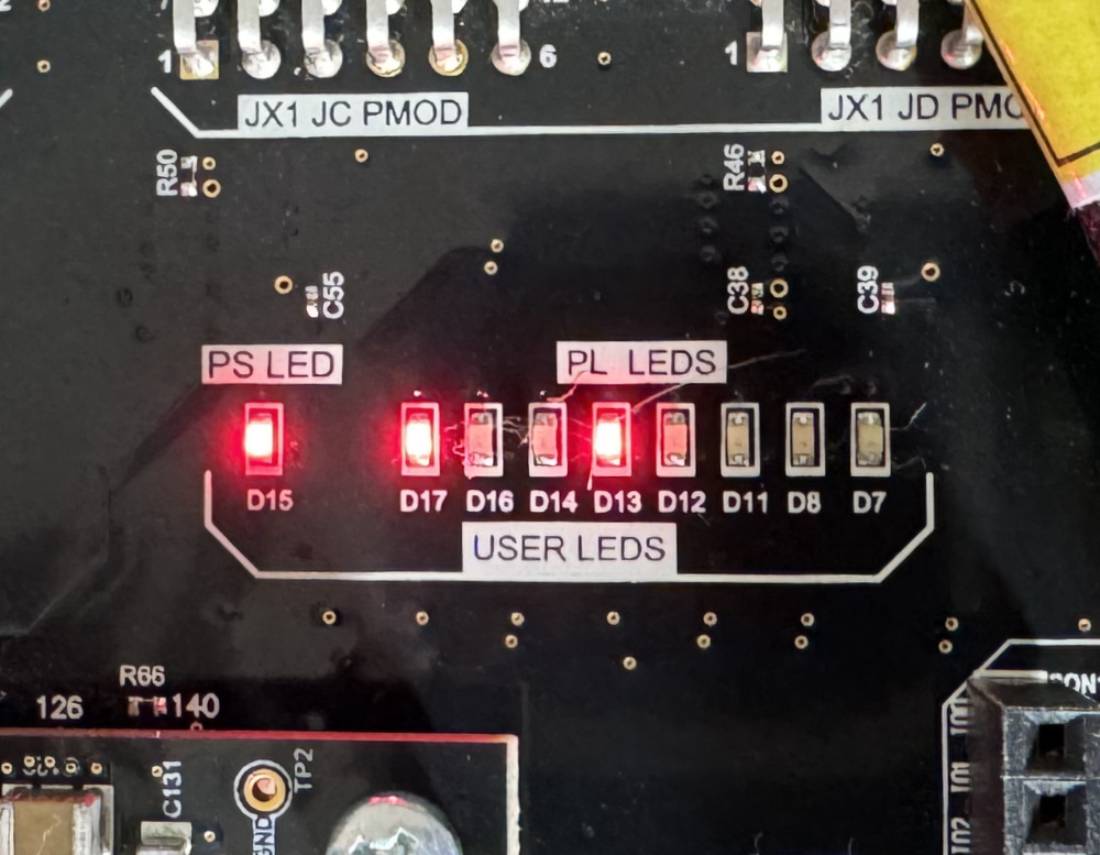
The register of the AXI GPIO slave is 8 bits long, while each bit corresponds to one LED.
This concludes this tutorial on how to setup a Vivado and Vitis project for the Zynq UltraScale+ board using AXI slaves and addressing them in C code.
PS: if you want to leave Picocom press [CTRL]+[A] and then [CTRL]+[X] in the terminal in which Picocom is running
Complete C Program Code
1
2
3
4
5
6
7
8
9
10
11
12
13
14
15
16
17
18
19
20
21
22
23
24
25
26
27
28
29
30
31
32
33
34
35
36
37
38
39
40
41
42
43
44
45
46
47
48
49
50
#include <stdio.h>
#include "platform.h"
#include "xil_printf.h"
#include "xparameters.h"
#include "xbasic_types.h"


int main() {
    init_platform();

    print("Hello World\n\r");

    // Address AXI slave test
    volatile Xuint32* axi_slave_test_baseaddr_p = (Xuint32*) XPAR_AXI_SLAVE_TEST_0_S00_AXI_BASEADDR;

    volatile Xuint32* axi_slave_test_reg_0_p = axi_slave_test_baseaddr_p;
    volatile Xuint32* axi_slave_test_reg_1_p = axi_slave_test_baseaddr_p+1;
    volatile Xuint32* axi_slave_test_reg_2_p = axi_slave_test_baseaddr_p+2;
    volatile Xuint32* axi_slave_test_reg_3_p = axi_slave_test_baseaddr_p+3;

    xil_printf("READ: axi_slave_test_reg_0 0x%x\n\r", *axi_slave_test_reg_0_p);
    xil_printf("READ: axi_slave_test_reg_1 %d\n\r", *axi_slave_test_reg_1_p);
    xil_printf("READ: axi_slave_test_reg_2 %d\n\r", *axi_slave_test_reg_2_p);
    xil_printf("READ: axi_slave_test_reg_3 0x%x\n\r", *axi_slave_test_reg_3_p);

    xil_printf("WRITE\n\r");
    *axi_slave_test_reg_0_p = 0xFF00FF00;
    *axi_slave_test_reg_1_p = 23;
    *axi_slave_test_reg_2_p = 42;
    *axi_slave_test_reg_3_p = 37;

    xil_printf("READ: axi_slave_test_reg_0 0x%x\n\r", *axi_slave_test_reg_0_p);
    xil_printf("READ: axi_slave_test_reg_1 %d\n\r", *axi_slave_test_reg_1_p);
    xil_printf("READ: axi_slave_test_reg_2 %d\n\r", *axi_slave_test_reg_2_p);
    xil_printf("READ: axi_slave_test_reg_3 0x%x\n\r", *axi_slave_test_reg_3_p);


    // Address PL LEDs
    volatile Xuint8* axi_gpio_baseaddr_p = (Xuint8*) XPAR_AXI_GPIO_0_BASEADDR;

    xil_printf("WRITE\n\r");
    *axi_gpio_baseaddr_p |= 0x1 << 4;
    *axi_gpio_baseaddr_p |= 0x1 << 7;

    xil_printf("READ: axi_gpio_baseaddr_p 0x%x\n\r", *axi_gpio_baseaddr_p);

    print("Successfully ran Hello World application");
    cleanup_platform();
    return 0;
}